Metal halide perovskites are emerging as front-runners in the realm of semiconductor materials due to their exceptional optoelectronic attributes. These materials boast high quantum yields for photoluminescence, impressive absorption coefficients, adjustable bandgaps, extensive carrier diffusion lengths, and a remarkable ability to tolerate defects. This unique combination of properties has captured the interest of researchers and industry experts alike, setting the stage for innovative advancements in optoelectronic applications.
Direct Laser Writing (DLW): A Groundbreaking Micro-Patterning Technique
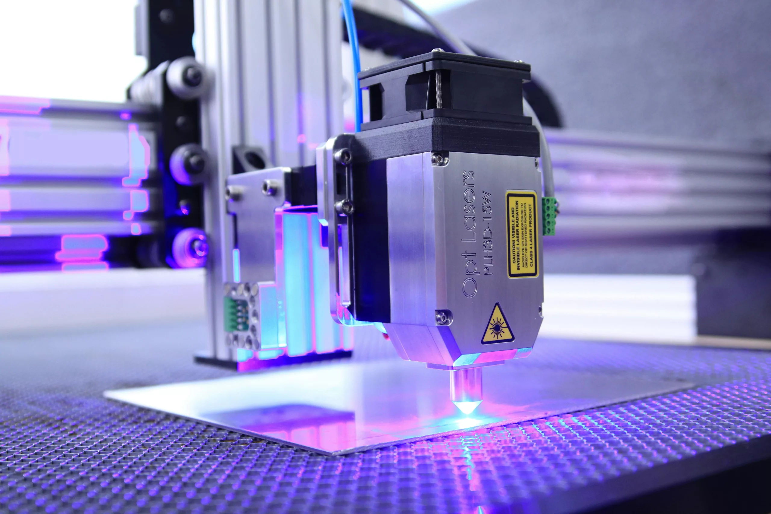
Direct Laser Writing is at the forefront of micro-fabrication technologies, offering a precise, non-contact, and maskless approach to patterning materials with microscopic detail. Utilizing a laser beam precisely focused through a high-resolution microscope, DLW achieves exceptional resolution that ranges from a few nanometers to a few hundred nanometers. The intricacies of this technique are influenced by the focal spot’s size and the material’s threshold response to the laser. DLW not only facilitates the creation of intricate patterns but also enhances our understanding of how light interacts with perovskite materials, ultimately leading to more efficient optoelectronic device designs.
Unlocking the Secrets of Laser and Perovskite Interactions
As explored in a detailed review paper by Professor Zhixing Gan and colleagues (DOI: 10.37188/lam.2024.004), researchers have been delving deep into the myriad ways lasers interact with perovskite materials. Six primary interaction mechanisms have been identified: laser ablation, induced crystallization, ion migration, phase segregation, photoreaction, and additional light-triggered transitions. These insights have paved the way to applying DLW to perovskites for creating micro and nano-patterned structures for a plethora of uses spanning displays, secure optical information, solar cells, LEDs, lasers, photodetectors, and even planar lenses, highlighting the patterned structures’ myriad advantages.
Potential and Challenges of DLW with Perovskites
Lasers serve as a sophisticated tool to shape, construct and process nano and microstructures on semiconductor surfaces. The unique composition of perovskites coupled with lasers’ capabilities offers a versatile platform for producing precisely controlled structures. The breadth of interaction mechanisms available to DLW signifies its potential across microelectronics, photonics, and optoelectronics. However, despite the considerable promise of implementing DLW with perovskites, obstacles persist. Challenges like improving resolution, extending the lifespan of separated phases, and adapting micropatterning to flexible substrates must be overcome to fully realize this technology’s potential.
Standing at the dawn of its development, DLW in perovskites is expected to experience a surge in demand and fundamental research in the foreseeable future. Anticipated applications of perovskite-based technologies cover an extensive range of optoelectronic and photonic arenas, including photon sources, micro and nanolasers, photodetectors, optical gates, communications, waveguides, and non-linear optics. The prospect of building and integrating photonic devices with diverse functionalities using a single perovskite chip signals a promising revolution in the field.
